Research
OPTICAL PROPERTIES AND QUANTUM EMISSION STUDIES OF METAL NANOCLUSTERS
Metal nanoclusters are made of a few to several hundred atoms of metal that exhibit unique optical and electronic properties. These properties arise from the size and shape of the nanocluster and the quantum confinement of electrons at the nanoscale. The optical properties of metal nanoclusters arise due to their strong interaction with light, which can be utilized in various applications such as sensing, imaging, energy conversion, quantum technology, etc.
The optical properties of metal nanoclusters are influenced by the size, shape, and composition of the nanocluster. For example, the absorption and scattering of light by a metal nanocluster depend on its size and shape, which determine its plasmonic resonance properties. Quantum emission studies of metal nanoclusters involve investigating the emission of photons from these nanoclusters. Metal nanoclusters exhibit unique quantum properties such as quantum confinement, surface plasmon resonance, and localized surface plasmon resonance, which make them promising candidates for applications in quantum optics and photonics. The emission of photons from metal nanoclusters and their charge transfer properties can be studied using various techniques such as single-molecule fluorescence microscopies, Stark spectroscopy, Raman scattering, etc.
In recent years, there has been significant progress in the development of metal nanoclusters with tailored optical and quantum properties. These advances have opened up new avenues for the design of nanoscale devices with enhanced functionality and performance. However, there are still many challenges that need to be addressed, such as understanding the fundamental photophysical processes underlying the optical and quantum properties of metal nanoclusters. In collaboration with the group of Dr. Rongchao Jin, we are trying to explore these fundamental science phenomena.
Electronic Properties of Molecules
Used for Opto-electronic Devices
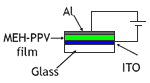
We measure several fundamental electronic properties of molecules such as charge transfer and electronic delocalization using a technique known as Stark spectroscopy. These measurements involve applying large electric fields to molecules in films or matrices and analyzing the effects of the field perturbation on the absorption or emission spectrum. Through these measurements, we pursue an understanding of how conformation and the environment, be it a protein, glass, polymer, or solvent, affects a molecule’s fundamental electronic properties. Equally important is how molecules interact with one another to form aggregate species having unique optical and non-linear optical properties, an area we are currently exploring. In collaboration with Dr. David Yaron, we have also exploited the interplay between computational chemistry and our experimental results to better understand the detailed interactions between molecules and their surroundings. In this area, we have recently focused on the properties of MEH-PPV and other molecules used to make to organic light emitting diode devices (OLEDs) and organic photovoltaic solar cells (OPVs). Stark spectroscopy not only allows us to determine how electronic delocalization may be enhanced by aggregation but also allows us to study the mechanism by which an applied electric field, such as those present in organic devices, can dissociate the excited state to produce free charges. In OLEDs, this process leads to emission quenching which is detrimental to device efficiency. However, as field-induced dissociation is the mechanism by which OPVs convert light to electricity, this process is important to the overall efficiency of the device.

Fluorescence Microscopy of Organic
Semi-conducting Materials:
From Single Molecules to Aggregates
Recent years has seen a huge growth in the types of organic molecules designed for molecular electronics including organic light emitting diodes (OLEDs) and photovoltaic cells (OPVs). Organic molecules have several advantages over conventional inorganic semi-conductors for these applications including the fact that they can be processed from solution to form flexible films and that elements of organic design can be used to tune properties such as brightness, stability, and the wavelengths of emission to produce devices that emit throughout the visible spectrum. One molecule of this type is the polymer MEH-PPV (see Fig. 1a) and its shorter-chain oligomers (see Fig. 1b). When these molecules are formed as thin films, as is necessary to fabricate devices, they typically form aggregates. Aggregates exhibit several desirable properties for device function such as protection from oxidative damage and enhanced charge transport. However, aggregation frequently shifts the wavelength of emission to lower energies and often significantly reduces its intensity. Both of these are undesirable from the standpoint of making organic films for lighting and display applications.
Our group is investigating the relationships between molecular structure (i.e. oligomer length and substitution patterns) and the brightness and photo-stability of molecules in the solid state, both in isolation (i.e. as single molecules) and as aggregates. Molecules that retain a high degree of brightness, even under aggregate conditions, would be good candidates to explore for molecular electronic devices. Through a systematic study of the effect of monomer chain length and aggregate size on photo-stability and brightness, we have identified several that exhibit favorable properties in the aggregate form.
The emission and morphological properties of these aggregates are characterized in bulk solution by a number of techniques including absorption and fluorescence spectroscopies, and fluorescence lifetime measurements. In addition, the properties of single aggregates are probed using single-molecule fluorescence microscopy, spectroscopy, and fluorescence lifetime imaging (Fig. 2). These imaging techniques reveal aggregate-to-aggregate variations in the emission wavelength, brightness, and lifetime. Moreover, we have shown that they are highly sensitive probes of interfacial regions within the aggregates that have distinguishable emission wavelength and lifetime properties (Fig. 3). We are now working to harness this potential to enable high-resolution imaging of thin films in device structures.
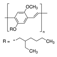
Figure 1a
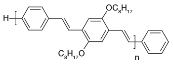
Figure 1b
Aggregates are groups of molecules that lie close together (typically within ~ 4 Å) in either well-ordered or disordered stacks. As a result, they interact with one another so strongly that the energies of their electronic states are different from those of the isolated molecules. These changes are seen as wavelength shifts in their absorption and emission spectra. Analysis of these changes yields information about the stacking arrangement of the molecules within the aggregate.
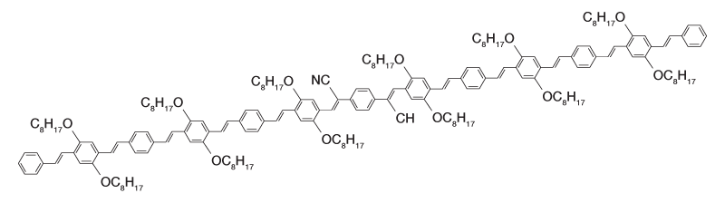
Figure 2a: Molecular structure of oligormeric CN-PPV.
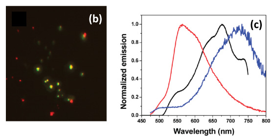
Figure 2b: False color microscopy image of red- and green-emitting CN-OPPV13 aggregates obtained by merging images obtained through 700/75 nm and 540/50 nm bandpass filters. (c) Averaged single aggregate emission spectrum (black) compared to spectra of the monomer(red) and aggregates (blue) in MeTHF/MeOH suspension. From J. Phys. Chem. C 2010, 114, 12078
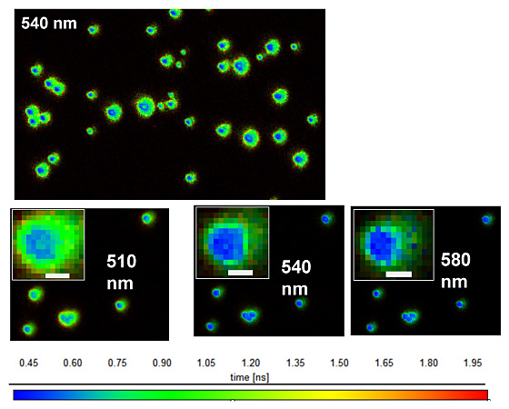
Figure 3: Fluorescence lifetime images of OPPV13 aggregates. Emission wavelengths are indicated (± 10 nm). Images are color coded by average emission lifetime (see scale at bottom of images). From J. Phys. Chem C 2011, 115, 15607
Single-Molecule Studies
of Heterogeneous Solvation in Ionic Liquids
Room temperature ionic liquids (RTILs) are a novel class of green solvents that have a variety of applications ranging from CO2 capture to use as battery electrolytes and in other energy storage devices. They are composed of organic cations and organic or inorganic anions, and have melting points below or near room temperature. RTILs have many desirable properties as solvents for organic reactions including low volatility, non-flammability, good thermal stability, and wide electrochemical windows. However, RTILs exhibit complex solvation dynamics that are still not well understood. For example, spectroscopic studies have shown that dye probes in RTILs exhibit multi-exponential decay dynamics and very broad absorption and emission spectra. This is taken as evidence that molecules within RTILs experience a wide variety of local environments with different solvation properties. Likewise, many simulations on RTILs have observed spatial heterogeneity caused by the aggregation of polar and nonpolar groups. To understand these phenomena at a detailed level, and how they impact the efficacy of ILs in the applications described above, we are studying their structure and solvation dynamics using single-molecule spectroscopy and molecular dynamics simulations through collaboration with the group of Dr. Hyung J. Kim. The single-molecule technique employed in this project is confocal fluorescence lifetime microscopy. Coupled with fluorescence correlation spectroscopy, using both lifetime- and wavelength-selective detection, confocal microscopy gives us the ability to study the local environment around each probe and the dynamics of each individual probe. Combining experiments with simulations, we will achieve a better understand of the interactions between the probes and the ionic liquids and the interactions between the components of ionic liquids themselves.


Energy Transfer
in DNA-based Dye Arrays
Our group is investigating the fundamental mechanisms giving rise to the unique and highly efficient energy-transfer properties of multi-chromophoric systems using bulk fluorescence and single-molecule fluorescence techniques including confocal and total internal reflection fluorescence microscopy. The goal is to engineer the light-harvesting potential and energy-transfer pathways using DNA as a scaffold to position multiple chromophores (dyes) in optimal positions. Such DNA nanostructures are a powerful method to construct well-defined arrays of fluorescent dyes which have many applications including biological labeling.
Examples of such arrays are the tetrahedral DNA nanostructure and three-way junction motif developed by our collaborators, the Armitage group. These have shown highly-desirable properties like high emissivity, photo-stability and compact size. Being a DNA nano-structure, the size and shape of the label can be easily tuned to match the requirements of each application. In addition, various dyes, including bis-intercalators and covalently-attached dyes are used to make multi-chromophoric arrays using DNA as the scaffold. When multiple dyes are involved a phenomenon known as Förster resonance energy transfer occurs between the two dyes. In this process, the excitation from one dye (the donor) is transferred to the other dye (the acceptor). This causes an increased spectral shift between the excitation light and the emitted light. These arrays are optimized to give the desired properties like brightness and spectral shift by varying the dyes used and their spatial arrangement.